Class 3: Amplifiers
Signal Generator
After finishing the signal generator circuit, test with the continuity function of a multimeter to verify that the things that need to be connected are connected and the things you do not want connected are not. You can use the lab’s adjustable power supply and oscilloscope to test the circuit. Solder a wire to Vcc and GND. Connect the other end of these wires to the adjustable power supply’s V+ and Gnd and set the power supply to 15V. Connect the oscilloscope to either E1 or E2 (remember, one is just the inverted version of the other) and GND as a reference. You should see an output signal like this:
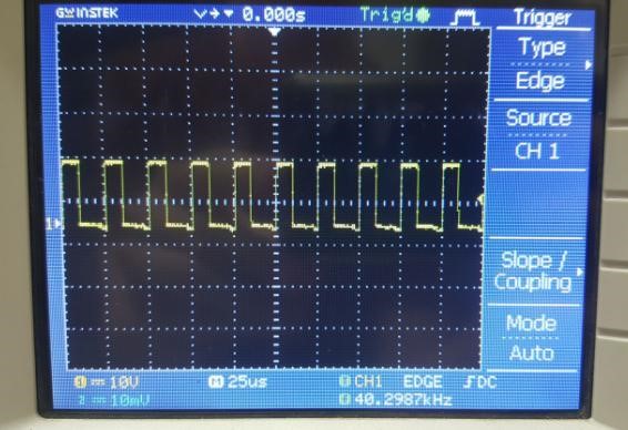
If you adjust the RT potentiometer, you should notice the frequency change. Try plugging in to the headphone jack and monitoring the output as well.
Amplifiers
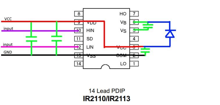
The output signal from the TL494 is not powerful enough to drive the MOSFET H-Bridge (don’t worry about this, this is discussed in the next class), so we must amplify the signal. We will be using the IR2110 IC (datasheet) to amplify our output signals. By inputting E1 and E2 from the TL494, we will receive a more powerful version of the same waveform for both. In addition, we require two copies of these waveforms as separate nodes for the H-Bridge. Thus, we need to use two amplifiers. We input E1 into the high input and E2 into the low input for amplifier 1. We input E2 into the high input and E1 into the low input for amplifier 2. Note that the inputs are switched for the two amplifiers. Do not worry about why we are doing this right now.
Here is the schematic of the amplifier circuit.
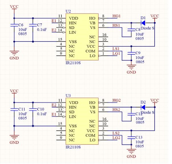
As you can see, E1 and E2 are connected to either high in or low in depending on which amplifier we are looking at. C6, C7, C10, and C11 are filtering capacitors as explained in the last class. We already have filtering capacitors between VCC and GND in the signal generator circuit, however it helps to have filtering capacitors physically close to the IC. That is the reason we include more in this circuit too. They are not strictly necessary, but help to keep the signal clean. VDD should connect to VCC and COM should be connected to VSS (GND). We include filtering capacitors C9 and C13 on the output side of the circuit for the same reason explained above.
D1 and D2 are diodes. A diode allows current to only flow in one direction. Think of the triangle as an arrow which points in the direction of allowed current flow. In this circuit, it allows current only to flow out of VCC. Because C8/C13 are connected to VCC, they will be charged to VCC. When there exists a voltage on Vs, for a brief moment the voltage at node Vb will be Vs + VCC (this is the same idea of how the MIDI capacitor functions from the signal generator). Because current flows from high voltage to low voltage, a current will want to flow from Vb to VCC. Having current flow in to the power supply VCC may cause damage to the power supply. For this reason, we include diodes D1 and D2 to prevent this. Current may only flow out of the power supply. Note for the diodes given out, the gray strip is the negative end of the diode (where the bar is in the diode symbol).
The labeled nodes HG1, HG2, HS1, HS2, LG1, LG2, LS1, LS2, will be used for the H-Bridge. Don’t worry about these yet, but think of these as our usable outputs.
Below is a diagram of how one might construct the circuit for one amplifier. The second amplifier should be constructed the exact same way but with the inputs swapped.